Recently, the Institute of Physics, Chinese Academy of Sciences/Beijing National Laboratory for Condensed Matter Physics (Microchip) Micro-processing Laboratory has made new progress in the controllable processing and optical applications of double-layered metal nanostructure arrays, mainly including the preparation of large-area double-layers. The controllable metal nanosphere array structure and the double-layered plasmonic supersurface structure have achieved breakthroughs in the highly sensitive Raman detection and control of the spatial freedom of light.
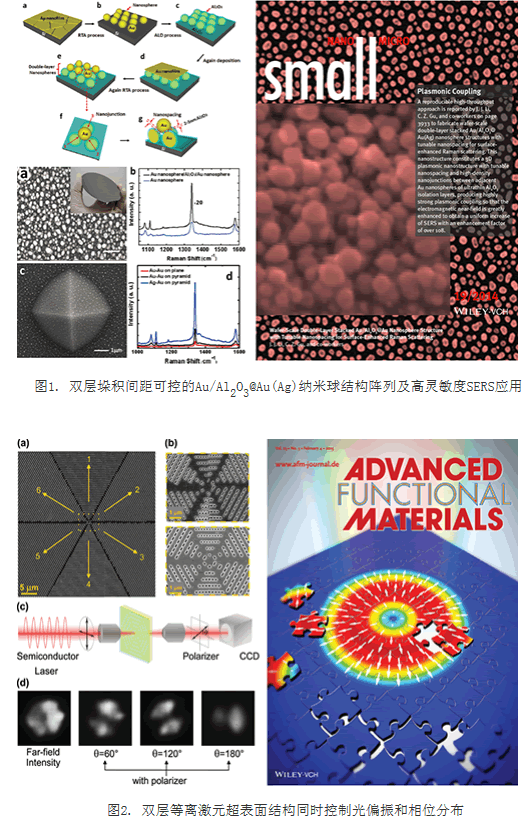
The noble metal nanoparticle array is the simplest plasmonic nanostructure. The plasmon coupling between adjacent metal particles can generate strong electromagnetic focusing and local field enhancement ("hot spot" effect), which can greatly improve The photoresponse, which is highly advantageous for high-sensitivity surface-enhanced Raman spectroscopy (SERS) detection applications, has attracted much attention. Because the adjacent position of noble metal nanoparticles is the key to the strong plasmon coupling effect, how to accurately regulate the size and spacing of metal particles has become the focus of research. At present, the chemical preparation method of sol metal particles has achieved the control of the morphology of metal nanoparticles to a certain extent, but it still has a comparative advantage in accurately controlling the adjacent spacing, overcoming the easy agglomeration, keeping the background clean, and evenly preparing the wafer size. Many problems are difficult to solve, so controllable preparation remains a major challenge.
At present, Hu Zhaosheng and Li Junjie of the Micro Processing Laboratory and researcher Gu Changzhi have proposed a physical preparation method for controlling the adjacent positions of precious metal nanoparticles, achieving precise control of particle size and spacing, and the spacing can be controlled within ~5 nm. The method combines electron beam deposition, rapid annealing technology and atomic layer deposition (ALD) technology to successfully prepare a Au/Al2O3@Au Au nanosphere array structure with controllable dual-pitch agglomerated spacing, wherein the nanosphere pitch is formed by an ALD deposition dielectric layer. The thickness is precisely controlled (1 to 10 nm). The research results show that this kind of lamination Au nanospheres with controllable spacing constructs a three-dimensional plasmonic nanostructure. The adjacent nanospheres are isolated by a ~5 nm dielectric layer and can generate a strong plasmon coupling effect. The local electromagnetic field intensity, further optimized and modulated by heterogeneous nanospheres (Au/Ag) and pyramidal array structure substrates, can increase the field enhancement factor (EF) by nearly four orders of magnitude (EF=~109). The nanostructure processing method is simple, high-efficiency, easy to control, non-polluting, can be patterned and the wafer size is uniformly manufactured, and is suitable for ultra-sensitive Raman detection and molecular electronics and photonics fields. This result was published as an animated headline on Small, 10 (2014) 3933.
Polarization and phase are two basic properties of light. Accurate control of the two is an important issue in the study of the role of light and matter. The traditional method is to use the birefringence and total internal reflection phenomenon of light in crystals and polymers to realize the control of the polarization state of light, relying on the geometry of the material and the design of the spatial distribution of the refractive index to realize the control of the light wavefront, only through The combination of multiple discrete optics enables simultaneous manipulation of the polarization and phase distribution of light. At the same time, the traditional optical devices are bulky and have a narrow spectral response, making it difficult to achieve system miniaturization and integration, and also unable to meet the needs of emerging technology development. Recently, it has been reported that the anisotropy of the plasmonic metamaterial structure is used to achieve the gradual gradient distribution of the optical phase at the interface and the conversion of the polarization direction of the linearly polarized light, but how to control the polarization direction and phase distribution of the light at the same time. It is still a difficult problem to solve.
In response to this problem, Li Junjie, Yang Haifang, and Gu Changzhi of the Microfabrication Laboratory collaborated with Nankai University and the Los Alamos National Laboratory in the United States to design and use nanofabrication techniques to prepare a dual-layer plasmon super surface material. The transmitted light phase and polarization direction of the sample are controlled simultaneously. This material can realize the control of the transmitted light phase through a large range of alignment and misalignment between two layers without changing the polarization. At the same time, the use of a polarization-selective transmission property of a rectangular hollow structure realizes the control of the polarization direction of transmitted light. A light field with arbitrary light polarization and phase distribution. This structure shows that the polarization-controllable broadband anomalous refraction phenomenon well characterizes the optical properties of the plasmonic superstructure, and further uses this structure to generate a radial vector beam. The plasmonic super-surface material proposed by the research results expands the degree of freedom of light control and has a very wide application in the field of photonics. This result was published as Back Cover on Adv. Func. Mater., 25 (2015) 704–710.
The above work was funded by the Ministry of Science and Technology, the National Natural Science Foundation of China, and the Chinese Academy of Sciences.
Sheet & Pipe Plasma Cutting Machine mainly for 3 axis 2D drawing cutting and round pipe cutting
1.This design fit for multifunction cutting requirements: both metal sheet and pipe cutting
2. Accept OEM for any pipe cutting diameter and working length. ( Normally from 100mm up to 600mm dia. )
3. Accept OEM for any table size: likes 4x4, 4x8 Plasma Cutting Table
4. Accept any materials cutting: Iron plate, Stainless steel plate, Titanium plate, Galvanized sheet, Aluminum plate, High speed steel etc
Steel Pipe Cutter,Sheet Cutting Machine,Metal Sheet Cutting Machine,Stainless Steel Cutting Machine
Jinan Huaxia Machinery Equipment CO.,Ltd , https://www.cnformingmachine.com